Writeup of the Secure Digital challenge
Performing signal analysis on a microSD card.
Intro
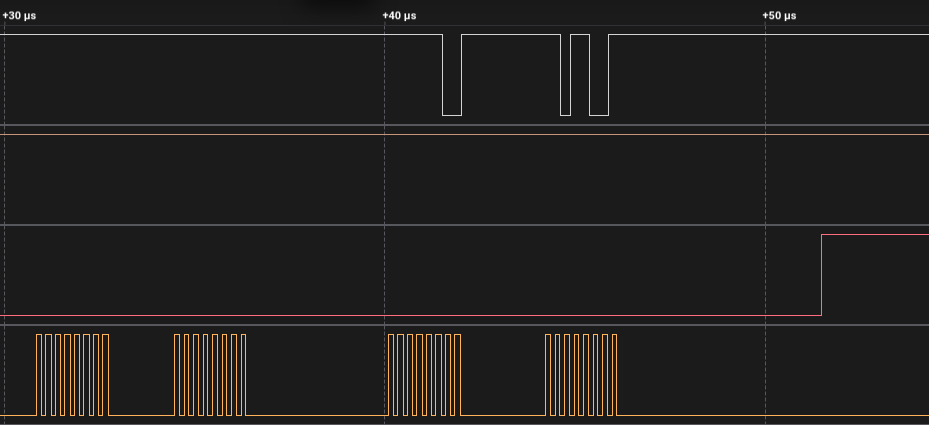
The challenge scenario highlights that we have a capture of the communication between a microSD card and the underlying system:
We must retrieve the master key stored on the microSD card that is inside the access control system. The traces connected to the card module are accessible on the top layer of the PCB. This enabled our operative to cut the traces and input a logic capture device in-between them. They could then trigger the read operation of the key that is transmitted over this unprotected serial interface. Can you find out what was read by the microSD card?
Our goal is to retrieve the key (flag) from a digital signal. The challenge is similar to the Unique challenge, so the approach will be very similar.
The Challenge
Download the challenge file and extracting the contents results in a file named trace_captured.sal. Opening the file inside the Logic2 analyzer results in the following signals:
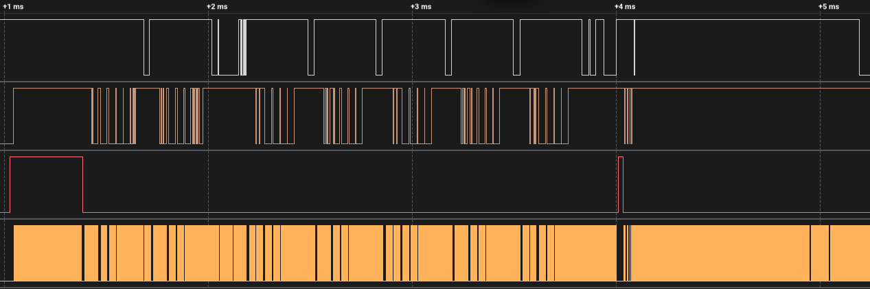 Signals inside the capture.
To decode the signals, we need to know what protocol the microSD card was talking. We can figure this out from the challenge intro, where is says the following: unprotected serial interface. This would imply that the communication protocol used was SPI (Serial Peripheral Interface).
Luckily, Logic2 has a SPI analyzer:
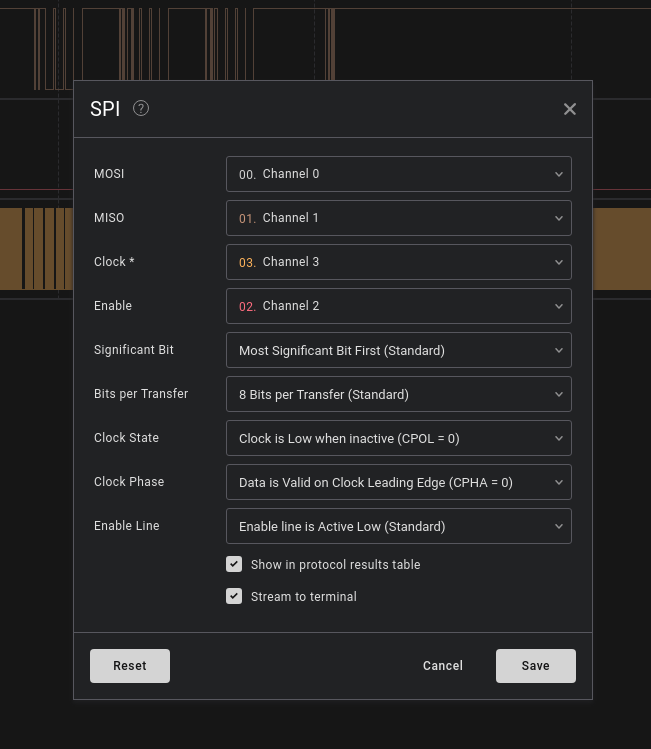 SPI analyzer settings.
Each signal corresponds to one function:
- The 1st signal corresponds to the MOSI (Master Out Slave In) signal
- The 2nd signal corresponds to the MISO (Master In Slave Out) signal
- The 3rd signal corresponds to the Enable signal
- And the 4th signal corresponds to the Clock signal
I’ll cover each signal more in the Extra Mile section. After applying the analyzer, the signal should look like this:
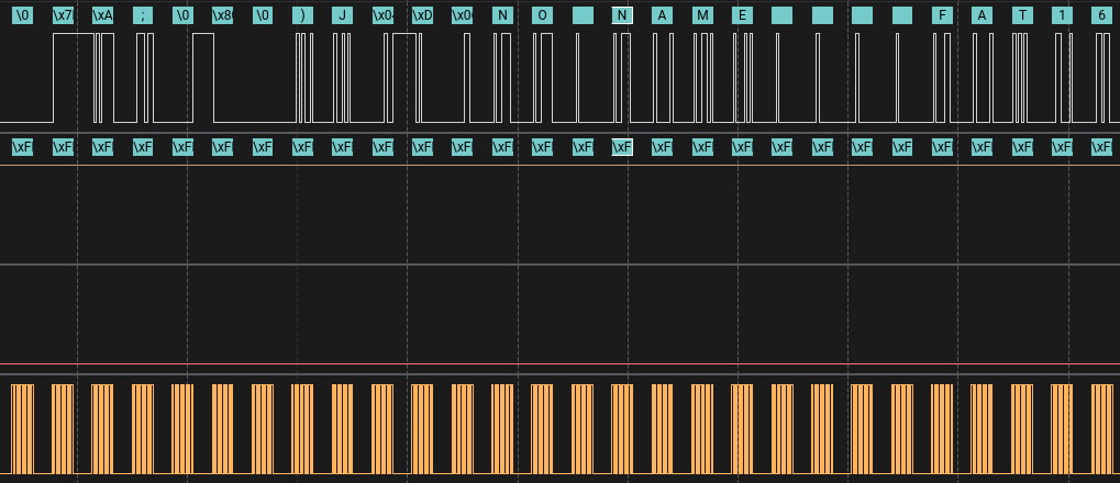 Decoded signal with ASCII text shown.
Now that we have the plain text communication, we can export it to a file and do some command line magic to extract the key (flag):
cut -d ',' -f 4 data.csv | tr -d '\n\"' | grep -o 'HTB{[^}]*}'
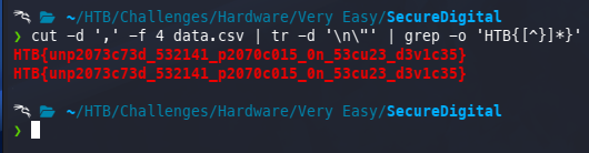 Extracted flag.
Resulting in the flag being: HTB{unp2073c73d_532141_p2070c015_0n_53cu23_d3v1c35}.
With the challenge being solved, let’s go the extra mile and figure how to determine what each signal is.
Extra Mile
While I mostly guessed about what each signal meant using the analyzer, I wanted to use this opportunity to learn how to identify what each signal is.
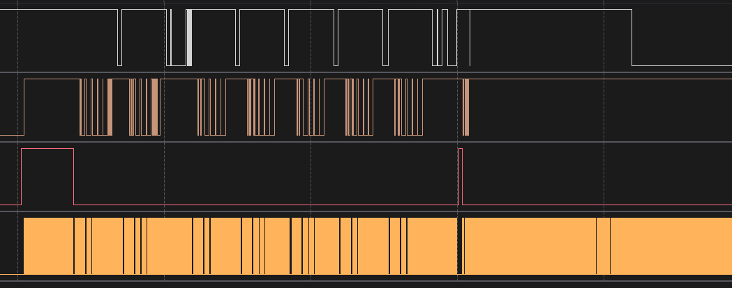 Additional look at all four signals.
From the image it’s clear that the last signal is the Clock signal due to the frequency. The Clock signal is used to synchronize the data transfer.
The second to last signal is also clearly the Enable (CS/SS/nSS) signal. This signal is used to select a device and when it’s pulled down to 0, the selected device is woken up. The signal remains pulled down to 0 during the entire data transfer window.
The last thing to determine what signal is MOSI and MISO. It turns out that for decoding the data…it doesn’t matter. Both the 1st and 2nd signal can be set to be MOSI or MISO and they will yield the same data. The data transferred between the SD and the PCB remains the same, MOSI/MISO only help determine the direction the data traveled. For proof you can see that setting the first signal to MOSI/MISO and the second to MOSI/MISO results in the same decoded data:
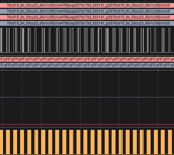 Same decoded data.
And that would be all for this challenge, catch you at the next writeup.